
A fully-functioning, DIY, self contained, built from scratch memory unit for the FRG-7700!
I'm calling it the NMU-7700.
I'll write the whole thing up properly later - with circuit and software descriptions and everything - but for now here's a quick demo video, a rundown of current features, potential features & expansion, and a short how-it-works.
Current Features
- 12 memories (same as the original): expandable to … well, lots. If you really wanted to, you could push it out to 32kbytes / 5 bytes per memory = over 6,500 (but it's up to you to figure out how to select them!)
- Fine tuning: like the MU-7700, the NMU-7700 enables the fine tune control on the front panel. Step-size is dependent on the accuracy of the existing front-panel control, but should typically be 15~20Hz.
- Frequency-accurate memories: the original MU-7700 stored frequencies with only 1kHz resolution, while the NMU-7700 stores frequencies with 6.25Hz resolution. This is particularly handy for CW, SSB, and other narrow-band & digital signals.
- Overall frequency accuracy is typically ±30Hz (worst case is ~±150Hz).
Potential Features / Expansion
These are the ideas I'm considering:- 128 memories: 'split' the 12 memory positions between 8 global all-band (independent of the band switch position) and 4 local per-band (dependent on the position of the band switch when the MR button is pressed) entries, increasing the number of memories without any hardware modifications. This would give (8 + (4 * 30) = 128 memory channels.
- External memory switches could be connected to the I2C buss via port expander ICs, to expand the number of available memory positions.
- Computer control via the serial port.
- Direct frequency entry via an add-on keypad / LCD connected to the I2C buss.
Hardware / How It Works
 |
| Interface board connections |
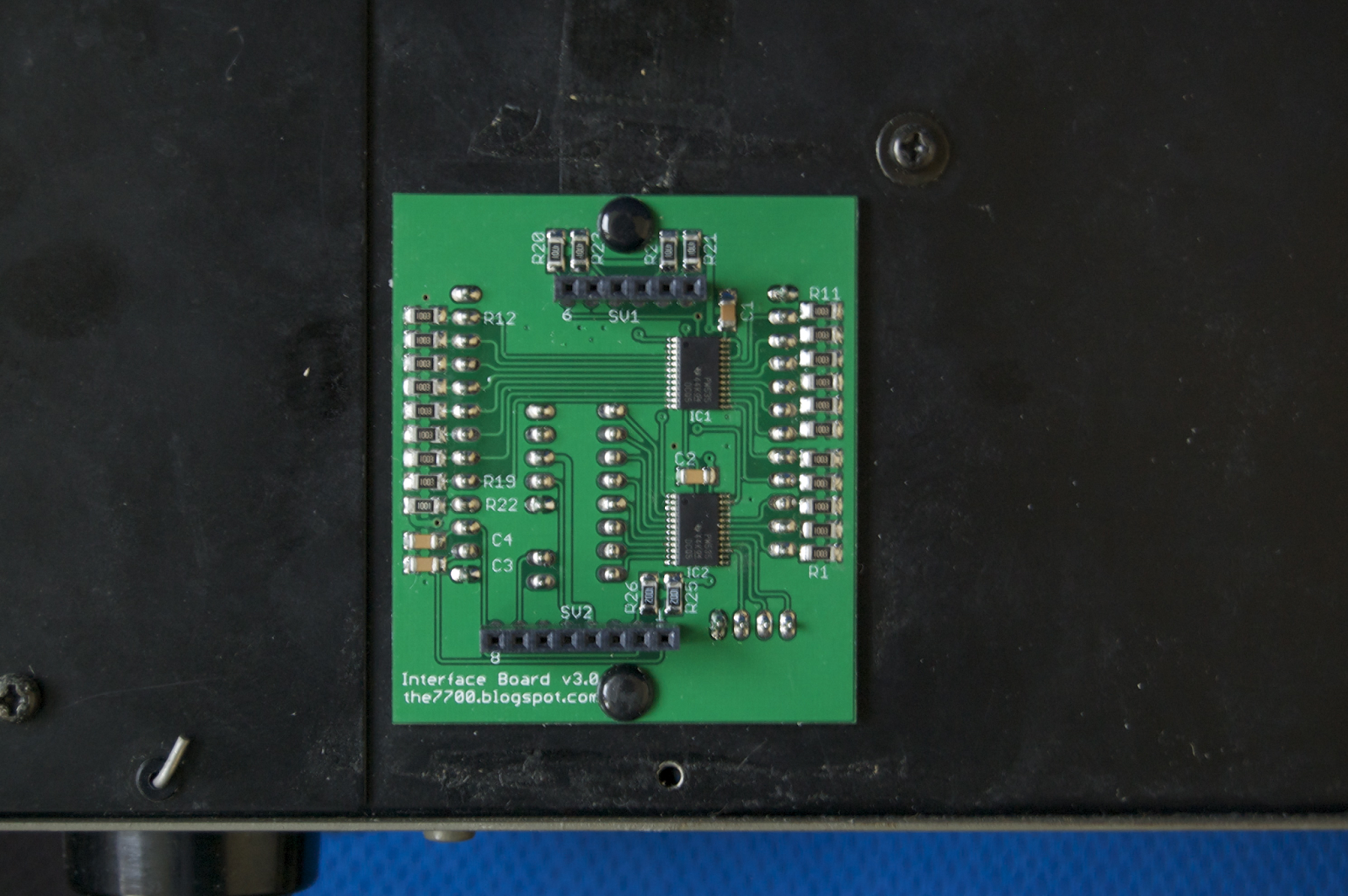 |
| Interface board, installed |
 |
| Main Board v4 |
- a 5v power supply (REG1, a 78M05 regulator) for both the main and interface boards ,
- an input buffer (IC2, a LMV761 comparator) for the frequency counter,
- a buffer/conditioner (IC3, a LM321 op-amp) for the fine-tune control,
- a DDS signal generator (IC4, a AD9833), driver amp (Q1 & Q2, 2N2222A transistors), and output filter for the memory unit VFO,
- a 24LC256 EEPROM (IC5) for memory storage, and
- an Atmel ATmega328 microcontroller (IC1), which controls the whole show.
When the "MR" button is pressed it disables the radio's band switch and tuning dial VFO, and sends a logic low to the micro. The software then …
- reads the memory switch and calculates the memory address,
- retrieves the band and VFO frequency from the EEPROM,
- writes to the I/O board to selects the correct band, VCO, and front end-filter on the radio, and
- programmes and enables the DDS to generate the stored VFO frequency
Simple, huh!
As is probably obvious, the software running on the microcontroller is the key to the whole thing. The ATmega328 is the same microcontroller as used in the Arduino Uno and similar boards, and the software for the memory unit has been developed using the Arduino environment.
(Errr... well, not quite! The Arduino IDE is tolerable for simple things, but it's bloody terrible for larger projects. The software has actually been written using embedXcode, an Arduino-compatible template for Mac OS X's Xcode IDE. Since it's Arduino-compatible, all I really need to do before release is to make sure it compiles and installs using the standard Arduino environment…)
The main difference between a standard Arduino Uno and the NMU-7700 is the clock speed - the Arduino runs at 16MHz, while the NMU-7700 runs at 20MHz (the maximum clock speed for the ATmega328, and the minimum practical speed for the DDS to generate 2.5-3.5MHz signals). In practice, all this means is that a modified version of the standard Arduino bootloader needs to be installed on the chip, and an entry added to the Arduino software's boards.txt file.
I think that's enough for now. Schematics for the interface and main boards are below; board files, software, and construction notes to follow soon!
 |
| Main Board schematic |
 |
| Interface Board schematic |
No comments:
Post a Comment